It's ALIVE! (SAMD21E18A, Assembly, No SDK)
This article is part of a series.
- Part 1: Hello LED on an AVR (ATtiny45) in C
- Part 2: How can I make programming an ARM chip as hard as possible?
- Part 3: How can I get this SAMD21E18 startup code a little sturdier?
- Part 4: This Article
- Part 5: And now for 3 ways to set an internal pullup
- Part 6: It'd make sense to do some toolchain clean up
Related Repo: https://github.com/carlynorama/StrippedDownChipRosetta/tree/main/ARM/SAMD21E18/03_AssmeblyBlink
More Refs
- YouTube: CMU Computer Architecture (18-447), Spring 2015 by Carnegie Mellon Computer Architecture If one wants to go off in the weeds? Taught by Prof. Onur Mutlu
-
YouTube:
Lecture 5: Memory Mapped I/O
(8:22) as part of
Short Lectures
by Embedded Systems and Deep Learning
Playlist for book by Yifeng Zhu
- Chapter 14: GPIO PDF of slides from above video by Dr. Yifeng Zhu for his 2018 class at the University of Maine
- YouTube: Raspberry Pi Pico Bare Metal Programming by Life with David I've only watched the first one but it looks excellent. Based on the RP2040
- GitHub: The samd port folder (5114f2c) in the micropython repo
Finding the GPIO Information in the Datasheet
Still this one
What Pin do we care about?
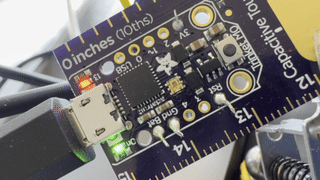
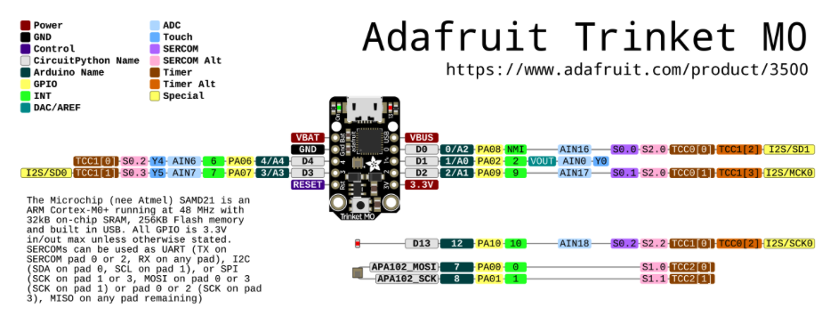
D13 == PA10
We aren’t trying to figure out how to lay out a circuit, we’re trying to figure out how to talk to the circuit we have. The PyRuler like many arduino compatible boards has a built in LED on “pin 13”. That means NOTHING to the SAMD21E18A. Going to the Adafruit docs on the Trinket M0, we can see that D13 matches to PA10.
What pins does the chip have?
When we write our code, what will be there to listen? What pins might have more than one purpose so if whe set a port up to do one thing it won’t do another?
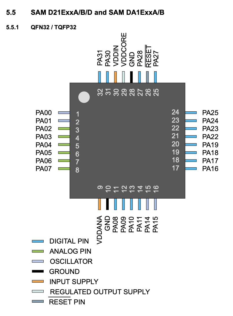
(Notice the number skipping compared the SAMD21J (5.1.1) , not all locations get a pin to the outside in this smaller package.)
What will this documentation call the GPIO peripheral?
PORT
Chip documentation uses a lot of abbreviations, steeped in history. Even though so many software packages call twiddling pins their GPIO library, an acronym, which you’d think would be perfect, don’t look for it in the datasheet. If you didn’t know about the history, how might you find out?
Section 6, Signal Descriptions List, gives us our list of acronyms for the type of electrical information the chip can take in and give out. Towards the end of the list we see “General Purpose I/O - PORT” Gotcha.
Generally speaking where will these values be in memory?
lowest value: 0x40000000
highest value: 0x42FFFFFF
We know from Figure 9-1, the memory map (shown last post) where the peripherals will be in memory memory map peripherals
Yeah but where are the PINS in there?
PORT 0x41004400
Table 12-1. Peripherals Configuration Summary Called PORT 0x41004400 (NOT GPIO) That puts it in the AHB-APB Bridge B section. This is where the “memory map” happens.
So thats where the pins are, Where and what do I call specifically to set them?
PA group offset 0x00 => 0x41004400
PB group offset 0x80 => 0x41004480
(from 23.6.2.2 Operation )
Everything we need is in section “23. PORT - I/O Pin Controller”, especially how to interact with the Memory Mapped I/O. As mentioned in the video above (Lecture 5: Memory Mapped I/O) there aren’t special port instructions at an assembly level on Arm chips, it’s all just memory instructions. Typically the chip manufacturers will provide special addresses to make certain operations faster. We can find them in
Table 23-7.
| Offset | Name | Acronym | Usage |
|---|---|---|---|
| 0x00 | Data Direction Values | DIR | 0 is input, 1 output |
| 0x04 | Data Direction Clear | DIRCLR | set to input with a 1 at bit, 0 no change |
| 0x08 | Data Direction Set | DIRSET | set to output with a 1 at bit, 0 no change |
| 0x08 | Data Direction Toggle | DIRTGL | toggled with a 1 at bit, 0 no change |
| 0x10 | Data Output Value | OUT | 0 is low, 1 is high |
| 0x14 | Data Output Clear | OUTCLR | set to low with a 1 at bit, 0 no change |
| 0x18 | Data Output Set | OUTSET | set to high with a 1 at bit, 0 no change |
| 0x1C | Data Output Toggle | OUTTGL | toggled with a 1 at bit, 0 no change |
| 0x20 | Data Input Value | IN | 0 is a low reading, 1 is a high reading |
| 0x24 | Input Sampling Mode | CTRL | 0 on demand sampling, 1 continuous sampling |
| 0x28 | Write Configuration | WRCONFIG | various meanings see 23.8.11 |
| 0x30 | Peripheral Multiplexing | PMUX | see 23.8.12 and Sec. 7 |
| 0x40 | Pin Configuration | PINCFG | various see 23.8.13, AND Table 23-2 |
What about when I want a to add a switch?
Remember for the ATtiny45 I had to set the pull up? Same for the SAMD21E18A. The configuration information lives in Table 23-2 (Pin Configurations Summary) and section 23.8.13 (PINCFG register details).
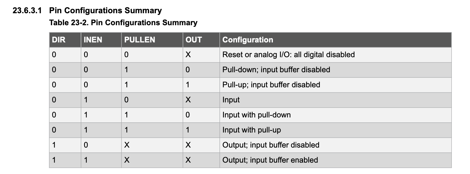
See 23.8.13
offset to pin settings == n*0x01 [n=0..31]
| 7 | 6 | 5 | 4 | 3 | 2 | 1 | 0 |
|---|---|---|---|---|---|---|---|
| DRVSTR | PULLEN | INEN | PMUXEN |
They’re a little tricky to use so lets do an example. Say I want a switch with logic low and a pull up resistor on PA05:
| Byte Address | Name | Value for Pin | Byte Address Calc | Which Bit | Meaning |
|---|---|---|---|---|---|
| 0x41004400 | DIR | 0 | PORT + DIR | 5 | Pin 5 is an output |
| 0x41004445 | DPINCFG05.INEN | 1 | PORTA + PINCONFIG + pin settings | INEN (bit 1) | Turn on the input buffer |
| 0x41004445 | DPINCFG05.PULLEN | 1 | PORTA + PINCONFIG + pin settings | PULLEN (bit 2) | Use a pull |
| 0x41004410 | OUT | 1 | PORT + OUT | 5 | That pull should be a pull up |
Delay Time
GCLK 0x40000C00
Default: 1MHz clock - OSC8M/8
Another thing I did with the ATtiny45 was check the clock settings. In Section 8.3.1, Starting of Clocks, the datasheet says - “the device will use a 1MHz clock. This clock is derived from the 8MHz Internal Oscillator (OSC8M), which is divided by eight.” Since that matches how I left the the ATtiny project, I’ll leave this chip alone.
Arm’s Cortex-M0+, the smallest of the family, offers more than one clock to it’s peripherals. That’s impressive. All of this is in Section 15 on GCLK, We’d have picked up from table 12-1 that all the offsets in this section are from GCLK 0x40000C00
What we want is in 15.7 the register summary and the follow up detailed pages.
| Offset | Name | Acronym | Usage |
|---|---|---|---|
| 0x00 | Control | CNTRL | Only bit 0, SWRST, software reset |
| 0x01 | Status | STATUS | Only bit 7, SYNCBUSY, Synchronization Busy Bus |
| 0x02 | Generic Clock Control | CLKCNTRL | WRTLOCK, CLKEN, GEN and ID |
| 0x04 | Generic Clock Generator Control | GENCNTRL | RUNSTDBY, DIVSEL, OE, OOV, IDC, GENEN, SRC, ID |
| 0x08 | Generic Clock Generator Division | GENDIV | 0 is low, 1 is high |
The key bits for inspecting that 1MHz clock:
GENCNTRL
Bit 20 – DIVSEL
Bits 12:8 - SRC
Bits 3:0 - ID
GENDIV
Bits 23:8 – DIV
Bits 3:0 - ID
Once I start loading code on the chip, I will use GDB to inspect the proper location.
Options for Blinking in Assembly
Assembly has different strategies than C. Try this fake-led blinking demo example first if you didn’t already.
I have two strategies I want to show. Both of these behave as if we only had the one address to use, the Data Output Value. SLOOOOW. The code on chip will be faster.
Explicit shifting and setting
.equ led_reg_addr, 0xff200000  // some archs have separate read and write addr

.equ onValue, 0x1     //will matter later because in real circuit 0 is frequently on
.equ offValue, 0x0
.equ pinLocation, 3

.equ delayTime, 3  // low number because I only step through on emulator

.global _start
_start:

	loop:
		MOV R3, #delayTime
		MOV R1, #onValue
		LSL R1, #pinLocation  //create the value
		LDR R0, =led_reg_addr
		STR R1, [R0]
		BL delay

		MOV R3, #delayTime
		MOV R1, #offValue
		LSL R1, #pinLocation
		LDR R0, =LED
		STR R1, [R0]
		BL delay

	BAL loop

delay:
	SUBS R3, R3, #1
	BNE delay
	BX LR
XOR Toggle
.equ led_add_reg, 0xff200000 //some archs have a
							 //different read and write
							 //address
.equ maskValue, 8
.equ delayTime, 3

.global _start
_start:

	ldr R5, =led_add_reg
	mov R6, #maskValue

	loop:
		LDR R4, [R5]  //if no one else will change the port or memory register (R4)
                      //and have no other reason to check port, potentially
                      //could skip the read and go with a desired initial value
                      //set before the loop and not do a full reload here. (just xor)
		EORS R4, R6 //XOR
		STR R4, [R5]
		LDR R3, =delayTime //instead of mov for future value
		BL delay
		B loop

delay:
	SUBS R3, R3, #1
	BNE delay
	BX LR
Now try it for real!
Finally! Whew.
Only one file has changed. The whole project reduces to an 11kb elf file.
.syntax unified
.cpu cortex-m0
.fpu softvfp
.thumb

.section .text.program_code

.equ portA_address, 0x41004400
.equ portA_DIRSET, 0x41004400+0x08
.equ portA_OUTTGL, 0x41004400+0x1C

.equ delayTime, 50000     //same clock speed as avr, so same value
.equ pinOffset, 10

.thumb_func
.global _start
_start:

	MOVS R4, #1
	LSLS R4, R4, #pinOffset  //R4 now contains the 1 at the pin offset bit.
                           //It should stay that way for the rest of the program

  //set the output pins
  LDR R5, =portA_DIRSET
  STR R4, [R5]


  LDR R5, =portA_OUTTGL  //R5 now points to the toggle-address
                          //It should stay that way for the rest of the program

  loop:
    STR R4, [R5]
    LDR R3, =delayTime
    BL delay

  B loop

.thumb_func
delay:
	SUBS R3, R3, #1
	BNE delay
	BX LR
Summary
Now was that so hard?
This article is part of a series.
- Part 1: Hello LED on an AVR (ATtiny45) in C
- Part 2: How can I make programming an ARM chip as hard as possible?
- Part 3: How can I get this SAMD21E18 startup code a little sturdier?
- Part 4: This Article
- Part 5: And now for 3 ways to set an internal pullup
- Part 6: It'd make sense to do some toolchain clean up